My first TTM Technologies role put me inside high-volume PCB manufacturing and set the foundation for the process engineering work I do now in Salem, New Hampshire.
DOEProcess EngineeringProductionValidation
Project visuals
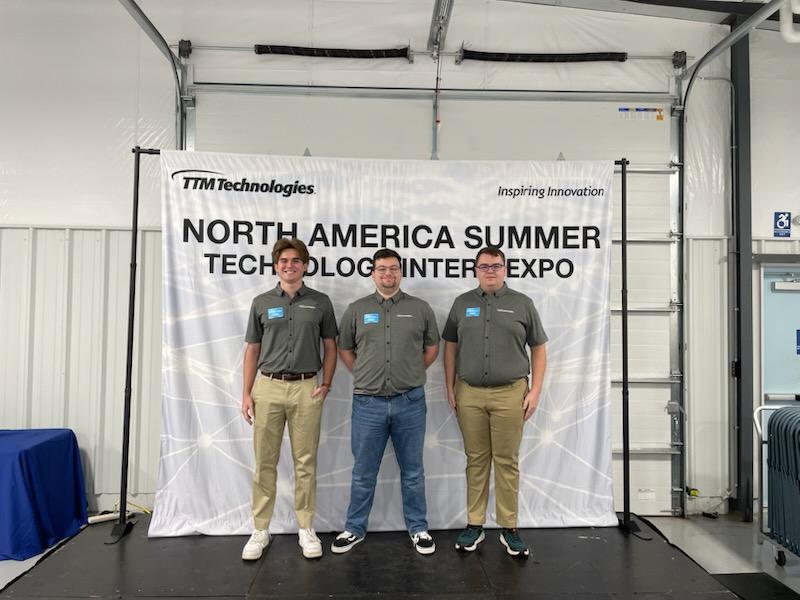
Intern expo
Photo from the TTM North America Summer Technology Intern Expo with the other interns at the end of the summer.
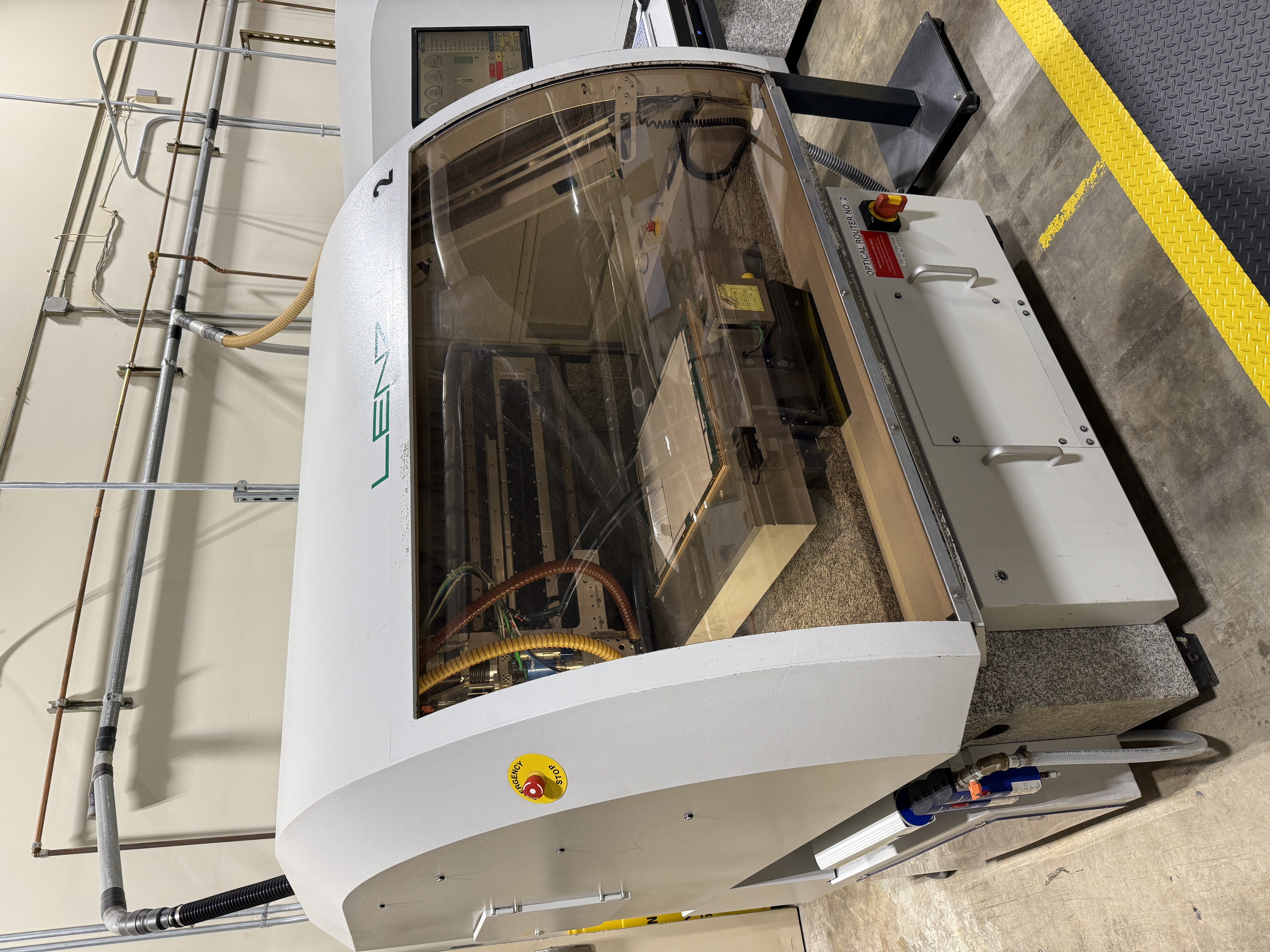
Optical router qualification
Optical router I helped qualify for production use.
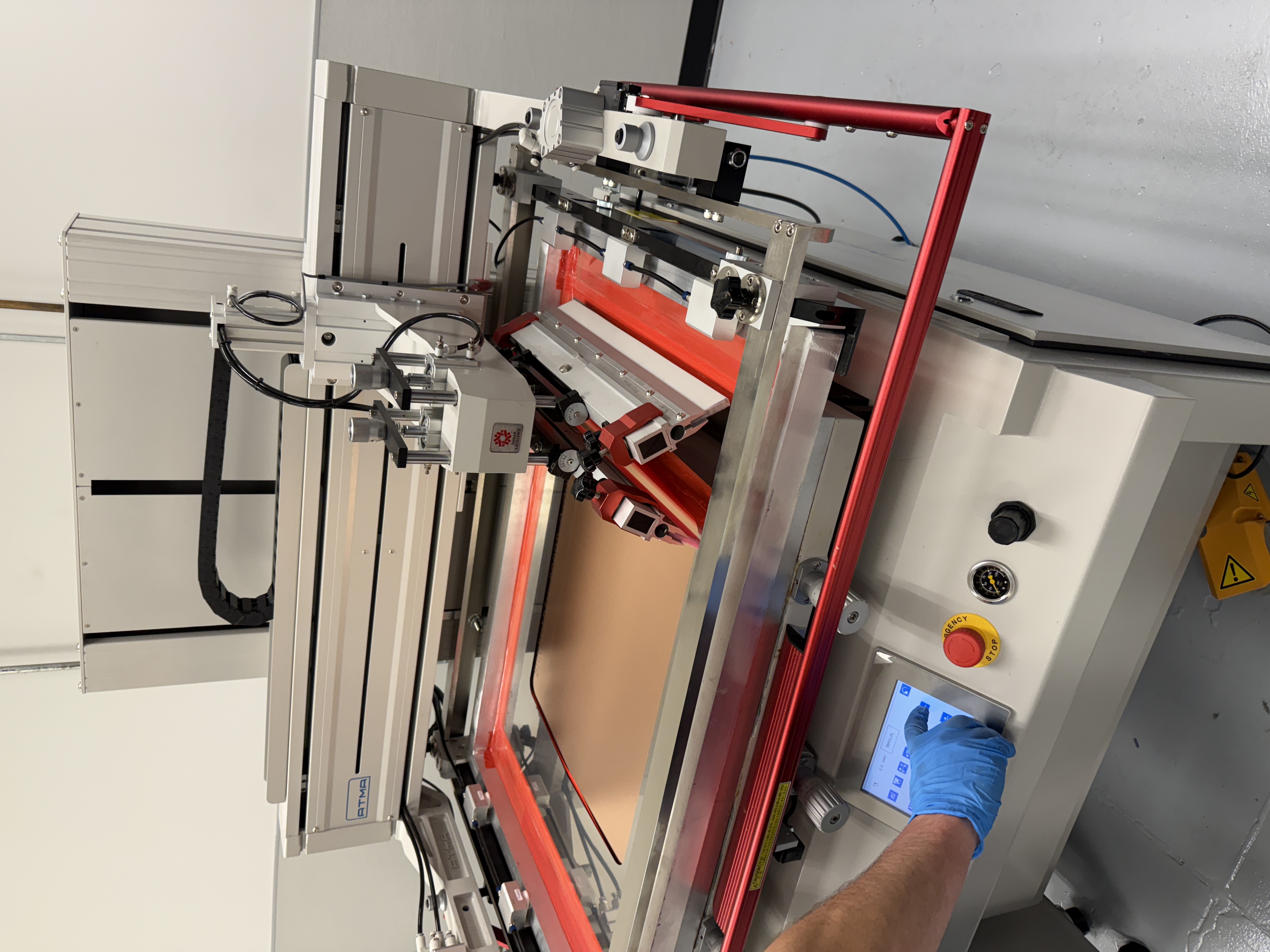
Design of experiments
Machine used in the DOE I ran to refine parameters for a new conductive paste manufacturing process.
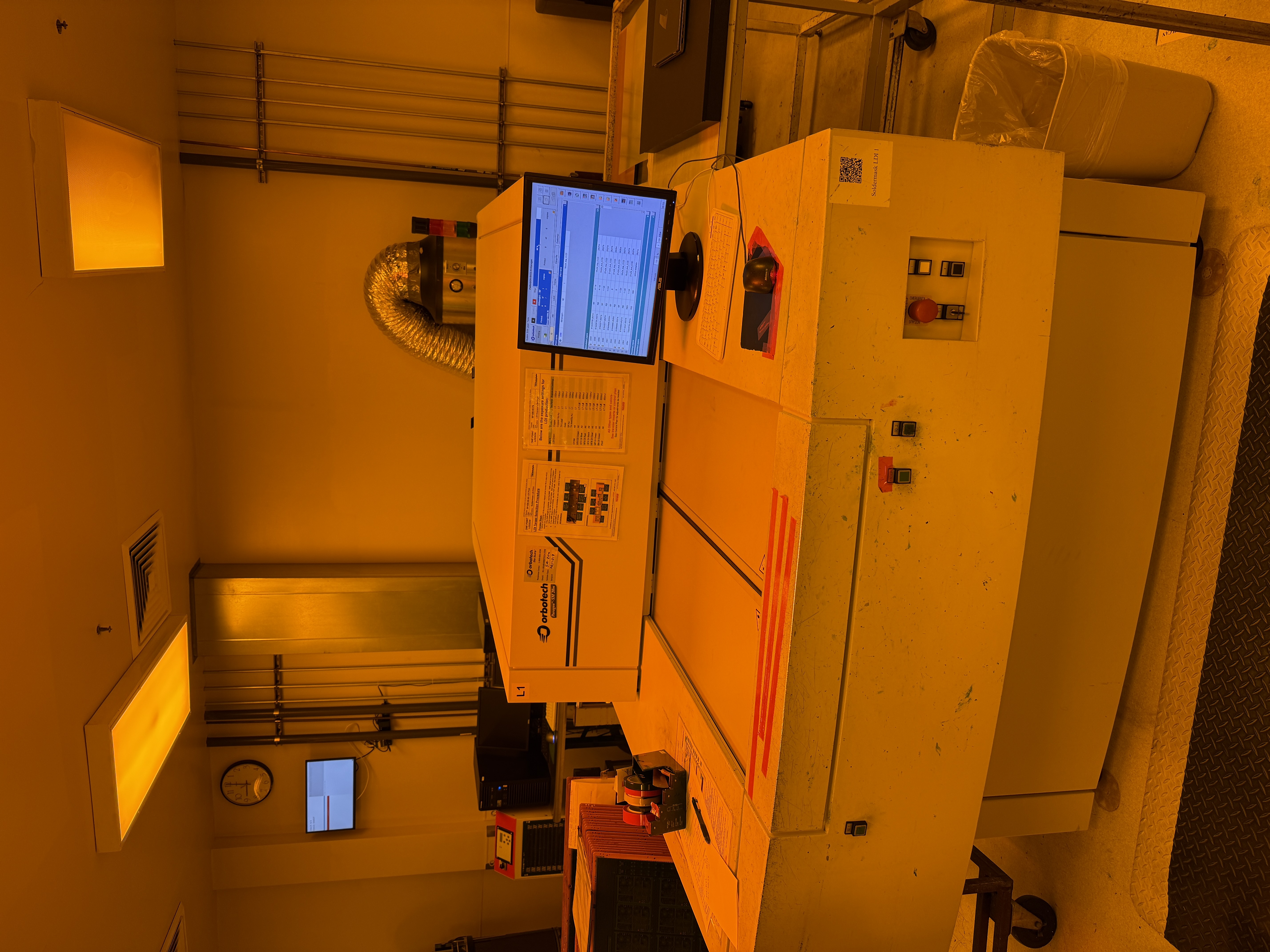
UV-sensitive film qualification
Laser direct imaging (LDI) machine used during the UV-sensitive film qualification work I supported for production implementation, helping reduce reliance on a single-point-failure process.
What I worked on
Supported DOE, process qualification, validation testing, equipment qualification, and manufacturing-data analysis in a high-volume PCB manufacturing environment.
Improved conductive paste yield by analyzing process data and refining key manufacturing parameters through DOE.
Reduced production risk by qualifying a backup UV-sensitive film process for a single-point-of-failure manufacturing path.
Expanded optical router capacity by qualifying a second machine for production use.